
Over the past two decades, nanoscience and technology has been extensively researched due to novel material properties, and potential for improvement of a variety of products in the electronics, photonics, energy-conversion, and biology fields. The initial phase of new material synthesis methods was followed by a second phase of demonstrating potential applications and uses for these materials. In the third phase, a major challenge is the development of new manufacturing processes to facilitate the transition of these technologies from the laboratory to the marketplace. This will require the development of scalable, low-cost manufacturing processes capable of synthesizing high quality materials with high throughput over large areas. Additionally, quality control on a manufacturing scale will require novel metrology tools capable of characterizing large quantities of nanomaterials in situ with high spatial and temporal precision. We have developed a variety of nanomanufacturing machines and processes, with an emphasis on low energy and raw material inputs, without the need for cleanroom processes such as photolithography, which can be substituted by scaleable technologies such as self-assembly or transfer processes. We also emphasize use of low-cost, flexible substrates compatible with processes such as roll-to-roll manufacturing, which has been identified as a key technology for reducing the cost of solar cells and other energy devices.
Selected Publications:
(10) B. A. Rorem, T. H. Cho, N. Farjam, J. D. Lenef, K. Barton, N. P. Dasgupta, L. J. Guo “Integrating Structural Colors with Additive Manufacturing Using Atomic Layer Deposition” ACS Appl. Mater. Interfaces 14, 31099 (2022) [link]
(9) A. J. Gayle, Z. J. Berquist, Y. Chen, A. J. Hill, J. Y. Hoffman, A. R. Bielinski, A. Lenert, N. P. Dasgupta “Tunable Atomic Layer Deposition into Ultra-High-Aspect-Ratio (60,000:1) Aerogel Monoliths Enabled by Transport Modeling” Chem. Mater. 33, 5572 (2021) [link]
(8) T. H. Cho, N. Farjam, C. R. Allemang, C. P. Pannier, E. Kazyak, C. Huber, M. Rose, O. Trejo, R. L. Peterson, K. Barton, N. P. Dasgupta, “Area-Selective Atomic Layer Deposition Patterned by Electrohydrodynamic-Jet Printing for Additive Manufacturing of Functional Materials and Devices” ACS Nano (2020) [link]
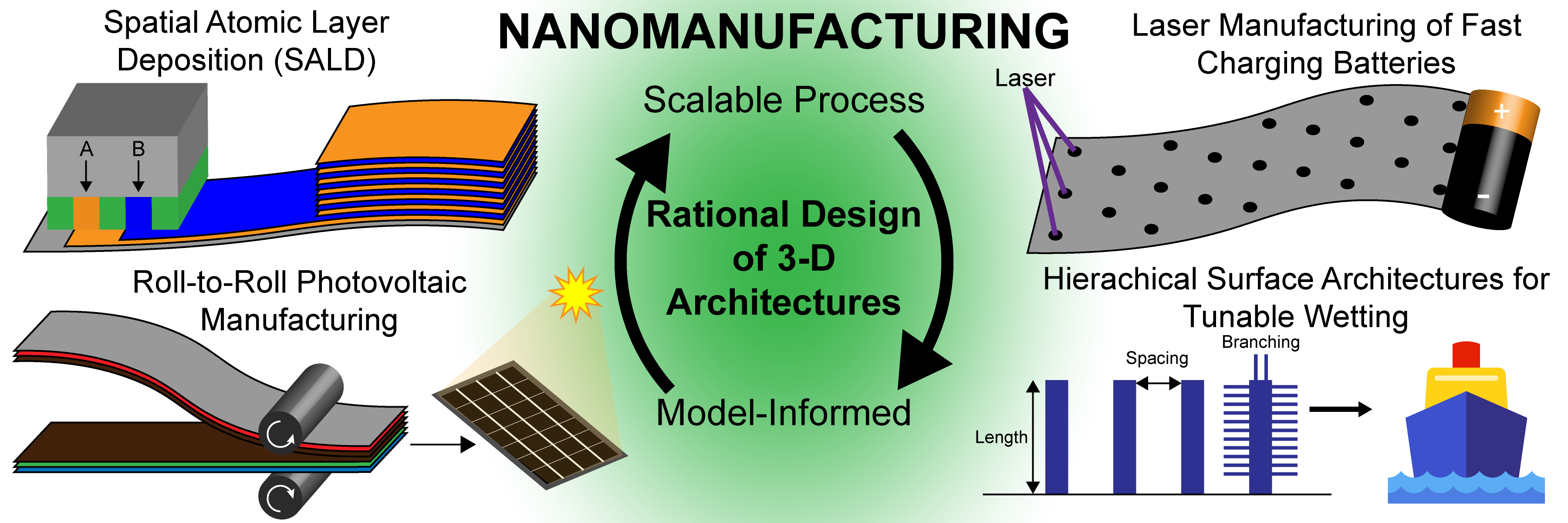
(7) J. Wang, S. Lee, A. R. Bielinski, K. A. Meyer, A. Dhyani, A. M. Ortiz‐Ortiz, A. Tuteja, N. P. Dasgupta, “Rational Design of Transparent Nanowire Architectures with Tunable Geometries for Preventing Marine Fouling” Adv. Mater. Interfaces 7, 2000672 (2020) [link]
(6) A. R. Bielinski, M. Boban, Y. He, E. Kazyak, D. H. Lee, C. Wang, A. Tuteja, N. P. Dasgupta, “Rational Design of Hyperbranched Nanowire Systems for Tunable Superomniphobic Surfaces Enabled by Atomic Layer Deposition” ACS Nano 11, 478 (2017) [link]
(5) A. R. Bielinski, E. Kazyak, C. M. Schlepütz, H. J. Jung, K. N. Wood and N. P. Dasgupta, “Hierarchical ZnO Nanowire Growth with Tunable Orientations on Versatile Substrates Using Atomic Layer Deposition Seeding” Chem. Mater. 27, 4799 (2015). [link]
(4) M. C. Langston, N. P. Dasgupta, H. J. Jung, M. Logar, Y. Huang, R. Sinclair and F. B. Prinz, “In Situ Cycle-by-Cycle Flash Annealing of Atomic Layer Deposited Materials”, J. Phys. Chem. C. 116, 24177 (2012). [link]
(3) N. P. Dasgupta, J. F. Mack, M. C. Langston, A. Bousetta and F. B. Prinz, “Design of an Atomic Layer Deposition Reactor for Hydrogen Sulfide Compatibility”, Rev. Sci. Instrum. 81, 44102 (2010). [link]
(2) W. Lee, N. P. Dasgupta, O. Trejo, J.-R. Lee, J. Hwang, T. Usui and F. B. Prinz, “Area-Selective Atomic Layer Deposition of Lead Sulfide: Nanoscale Patterning and DFT Simulations”, Langmuir 26, 6845 (2010). [link]
(1) N. P. Dasgupta, J. Sun, C. Liu, S. Brittman, S. C. Andrews, J. Lim, H. Gao, R. Yan and P. Yang, “Semiconductor Nanowires – Synthesis, Characterization, and Applications” Adv. Mater. 26, 2137 (2014). [link]