
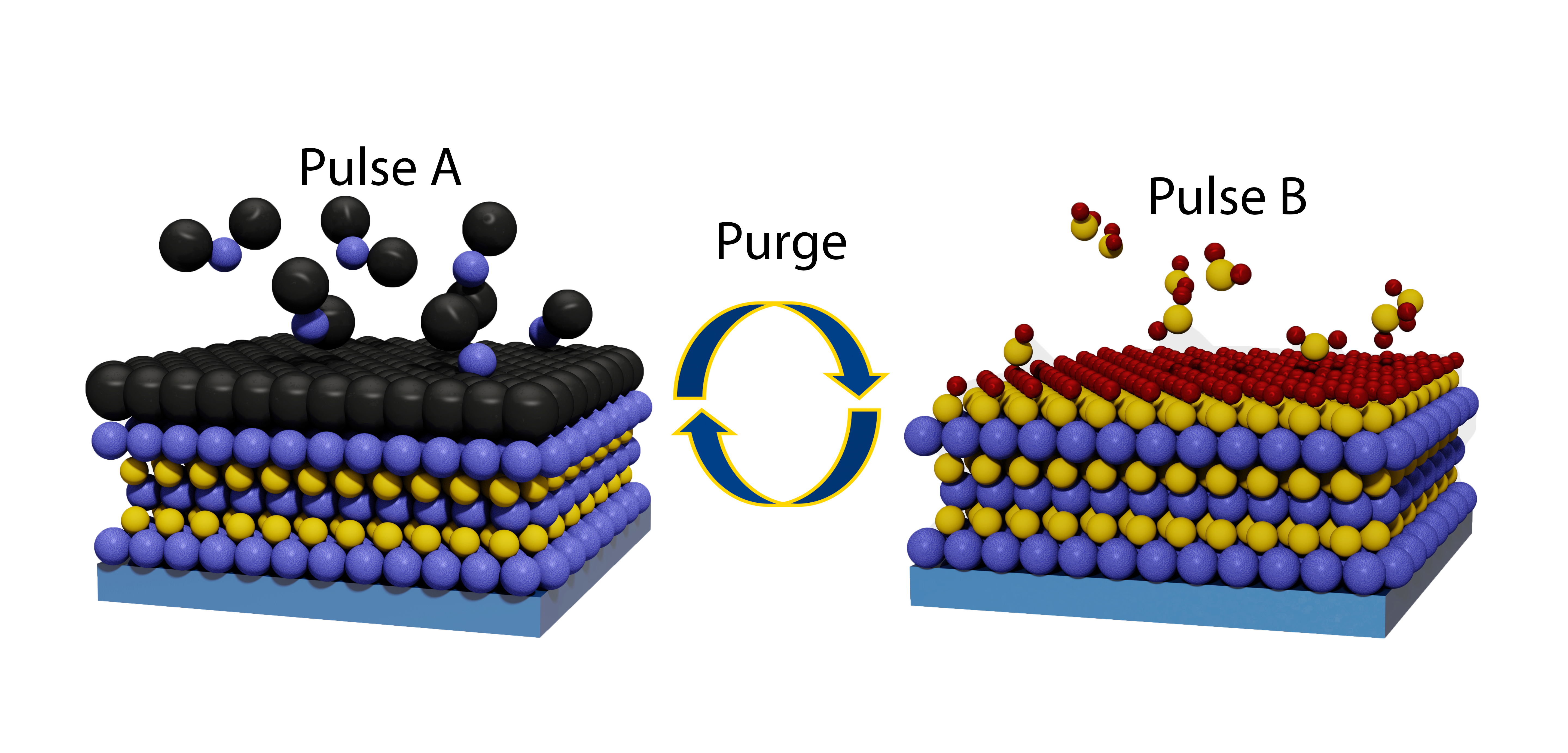
ALD is a modified chemical vapor deposition (CVD) process for depositing thin films or nanoparticles with sub-nm precision in feature size. ALD is based on the sequential exposure of a substrate to gas-phase precursor molecules, which poses the unique characteristic of self-limiting surface chemistry. This leads to saturation of the surface with a single layer of adsorbed molecules during each exposure, allowing for conformal coating of ultra-high aspect ratio surfaces. We have developed the capability to deposit a variety of metal oxide, metal sulfide, and metallic materials by ALD. By control of the nucleation behavior of the materials, either dense films or isolated nanoparticles can be deposited on a wide range of high surface-area structures. We explore ALD chemistry through high-resolution microscopy, spectroscopy, and quantum simulations to gain atomic-scale insight into the growth and properties of these materials. In particular, we are interested in applying ALD chemistry to engineer surfaces and interfaces of energy conversion devices, which are crucial for the kinetics of charge transfer processes.
Selected Publications:
(12) O. Trejo, T. H. Cho, S. Sainio, N. P. Dasgupta “XANES Studies of Zinc Tin Oxide Films Deposited by Atomic Layer Deposition: Revealing Process-Structure Relationships for Amorphous Oxide Semiconductors” J. Phys. Chem. C. 127, 338 (2023) [link]
(11) A. J. Gayle, Z. J. Berquist, Y. Chen, A. J. Hill, J. Y. Hoffman, A. R. Bielinski, A. Lenert, N. P. Dasgupta “Tunable Atomic Layer Deposition into Ultra-High-Aspect-Ratio (60,000:1) Aerogel Monoliths Enabled by Transport Modeling” Chem. Mater. 33, 5572 (2021) [link]
(10) J. D. Lenef, J. Jo, O. Trejo, D. J. Mandia, R. L. Peterson, N. P. Dasgupta, “Plasma-Enhanced Atomic Layer Deposition of p-type Copper Oxide Semiconductors with Tunable Phase, Oxidation State, and Morphology” J. Phys. Chem. C 125, 9383 (2021). [link]
(9) E. Kazyak, M. Shin, W. S. LePage, T. H. Cho, N. P. Dasgupta “Molecular Layer Deposition of Li-ion Conducting “Lithicone” Solid Electrolytes” (Invited Article for ChemComm Emerging Investigators Issue) Chem. Commun. 56, 15537 (2020). [link]
(8) T. H. Cho, N. Farjam, C. R. Allemang, C. P. Pannier, E. Kazyak, C. Huber, M. Rose, O. Trejo, R. L. Peterson, K. Barton, N. P. Dasgupta “Area-Selective Atomic Layer Deposition Patterned by Electrohydrodynamic Jet Printing for Additive Manufacturing of Functional Materials and Devices” ACS Nano 14, 17262 (2020). [link]
(7) C. R. Allemang, T. H. Cho, O. Trejo, S. Ravan, R. E. Rodríguez, N. P. Dasgupta, R. L. Peterson, “High‐Performance Zinc Tin Oxide TFTs with Active Layers Deposited by Atomic Layer Deposition” Adv. Electron. Mater. 6, 2000195 (2020). [link]
(6) O. Trejo, A. L. Dadlani, F. De La Paz, S. Acharya, R. Kravec, D. Nordlund, R. Sarangi, F. B. Prinz, J. Torgersen, N. P. Dasgupta, “Elucidating the Evolving Atomic Structure in Atomic Layer Deposition Reactions with in Situ XANES and Machine Learning” Chem. Mater. 31, 8937 (2019). [link]
(5) N. P. Dasgupta, H.-B.-R. Lee, S. F. Bent, P. S. Weiss, “Recent Advances in Atomic Layer Deposition”, Chem. Mater. 28, 1943 (2016). [link]
(4) N. P. Dasgupta, X. Meng, J. W. Elam and A. B. F. Martinson, “Atomic Layer Deposition of Metal Sulfide Materials”, Acc. Chem. Res. 48, 341 (2015). [link]
(3) N. P. Dasgupta, C. Liu, S. Andrews, F. B. Prinz and P. Yang, “Atomic Layer Deposition of Platinum Catalysts on Nanowire Surfaces for Photoelectrochemical Water Reduction”, J. Am. Chem. Soc. 135, 12932 (2013). [link]
(2) J. W. Elam, N. P. Dasgupta and F. B. Prinz, “ALD for Clean Energy Conversion, Utilization, and Storage”, MRS Bull. 36, 899 (2011). [link]
(1) N. P. Dasgupta, H. J. Jung, O. Trejo, M. T. McDowell, A. Hryciw, M. Brongersma, R. Sinclair and F. B. Prinz, “Atomic Layer Deposition of Lead Sulfide Quantum Dots on Nanowire Surfaces”, Nano Lett., 11(3), 934 (2011). [link]